
AI Is Being Powered by Tech That Looks Almost Alien
The machines behind every frontier model are not servers. They are vacuum chambers, tin plasma, mirrors polished to tens of picometres, and racks that drink as much power as a city block.
Part of theAI Stocks CenterFrom the Veritasium film The Closest Thing We Have to Alien Technology (31 December 2025). Notes at the end.
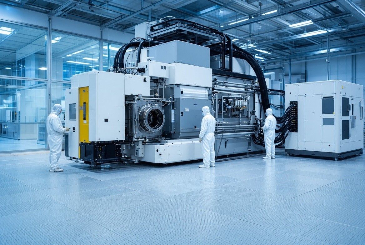
The machine that does not look like it belongs here
On the last day of 2025, Veritasium posted a film with a title that does the engineering a favour. The Closest Thing We Have to Alien Technology is not about a secret craft or a leaked patent. It is about a commercial tool, built in Veldhoven in the southern Netherlands, that prints the transistors inside the chips that train and run artificial intelligence. The film has since passed 60 million views. The reason is not the narration. It is the object.
Stand next to one and the science-fiction reflex is reasonable. The scanner is the size of a bus. It ships in on the order of a couple of hundred crates. Installation takes months and a small army of engineers. The optical path is a vacuum, because the light it uses is absorbed by air and by glass. Inside, fifty thousand droplets of molten tin a second are hit by a carbon-dioxide laser and turned into a plasma hot enough that popular accounts put it near forty times the surface of the Sun. The light that plasma throws off, at 13.5 nanometres, bounces off mirrors so smooth that ASML itself describes the largest of them as a one-metre optic whose deviations are tens of picometres: a playing card's thickness, if the mirror were scaled to the surface of the Earth.
None of that is a metaphor for how clever the software is. It is the manufacturing step without which the software has nowhere to run. NVIDIA does not print its own Blackwell dies. TSMC does, and TSMC, Samsung and Intel print the leading edge on tools only ASML sells. Pull the scanner out of the chain and the roadmap for denser logic, denser memory and cheaper inference stalls. The chatbot is downstream of a tin droplet.
This piece takes the film as the brief and then checks it. The alien impression is earned. Several of the round numbers in the narration are popular shorthand, and a few of them attach to the newest High-NA machine rather than to every EUV tool in the field. The physics is not. What follows is the machine, the sister machines that finish the AI stack, and a record of what is solid, what is industry-reported, and what the film compressed.
Why the chatbot is downstream of a tin droplet
A frontier model is a file of weights. Those weights are numbers, stored in high-bandwidth memory, multiplied by matrices on a graphics processor or a specialised accelerator, moved across a network, and cooled by a liquid loop that did not exist in a typical data-centre design ten years ago. Every one of those parts is a chip, or a stack of chips, and every leading-edge chip is a patterned wafer.
The pattern is the product. A logic die at a 3-nanometre-class or 2-nanometre-class node is not a flat circuit. It is a city of a hundred layers or more: transistors at the bottom, then contacts, then a thicket of metal interconnect, then the pads that will later be bonded to a package. The film's opening image, a chip that becomes a nanoscopic city when you zoom in, is the right picture. The wires on a modern die run for kilometres if you unspool them. The transistors at the bottom are the switches. Everything above them is plumbing for electrons and, increasingly, for the heat those electrons leave behind.
Training a large model is a memory-bandwidth problem wearing a compute costume. The arithmetic units starve unless the weights arrive on time. That is why the AI bill of materials is not "a GPU." It is a logic die, several stacks of high-bandwidth DRAM, a silicon interposer or a bridge that ties them together, a package substrate, a cold plate, a rack manifold, and a building that can feed the rack 120 to 140 kilowatts without browning out the row. Every layer of that stack was printed, etched, deposited or assembled on a tool whose precision is measured in atoms.
Lithography is the step that sets the minimum feature. Deposition lays down films. Etch cuts them. Implant dopes the silicon. Polish flattens the wafer so the next layer can be printed in focus. A leading-edge process can run well past a thousand process steps, and the lithography steps are repeated dozens of times. If the printer cannot resolve the feature, none of the later tools matter. That is the narrow sense in which one Dutch machine sits under the entire AI boom.
How a chip is actually printed
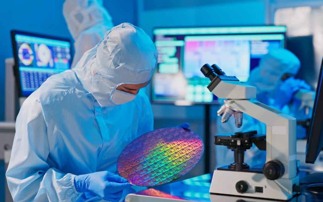
The starting material is sand, in the industrial sense: silicon dioxide, reduced and purified until the remaining impurities are counted in parts per billion. A seed crystal is dipped into molten silicon and withdrawn, pulling a single-crystal ingot. The ingot is sawn into wafers, today typically 300 millimetres across, then polished to a mirror. That wafer is a blank. The chip does not exist until the pattern does.
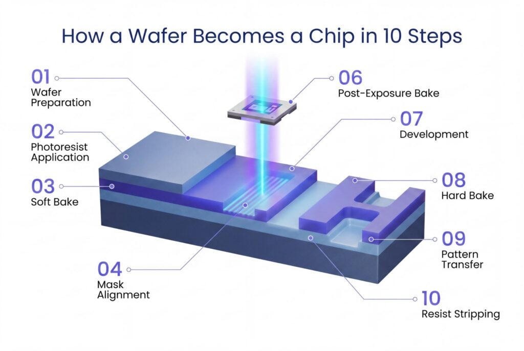
Patterning is a stencil process with unforgiving optics. The wafer is coated with photoresist, a polymer whose solubility changes when it is exposed to light. A reticle, the master stencil, carries the layer pattern. Light carries that pattern onto the wafer. The exposed resist is developed. Etch transfers the remaining pattern into the film underneath. The resist is stripped. The cycle repeats for the next layer.
The limit is diffraction. You cannot print a feature much smaller than the wavelength of the light you use, and you cannot cheat that limit forever by tricks alone. The working relation is the Rayleigh criterion: the minimum half-pitch scales with wavelength divided by the numerical aperture of the optics, multiplied by a process factor k1. For two decades the industry lived on 193-nanometre deep-ultraviolet light from an argon-fluoride excimer laser, pushed harder by immersion (a film of water between the lens and the wafer, which raises the effective numerical aperture) and by multi-patterning, which splits one dense layer into two, three or four exposures.
Multi-patterning worked. It also multiplied cost, cycle time and the ways a layer can miss its neighbour. By the middle of the last decade the industry had a choice. Keep subdividing 193-nanometre exposures until the overlay budget ate the yield, or change the wavelength. The change on the table was a drop from 193 nanometres to 13.5. That is not an incremental lamp swap. It is a different machine.
The wavelength that killed the lens
Thirteen-point-five nanometres sits in the extreme ultraviolet, on the edge of what used to be called soft X-rays. Air absorbs it. So does glass. So does the ordinary photoresist chemistry the industry had spent twenty years tuning. A lens, in the ordinary sense, cannot be the optic. The light never gets through it.
The workaround is a mirror, and not a metal mirror in the bathroom sense. EUV reflection is a Bragg stack: alternating layers of molybdenum and silicon, each a few nanometres thick, spaced so that the weak reflection from each interface adds in phase at 13.5 nanometres. A good stack reflects about 70 percent of the light that hits it at the design angle. The rest is absorbed as heat. There is no EUV equivalent of a lens that passes 99 percent.
Count the bounces. Light leaves the plasma, hits a collector, travels through an illuminator of several mirrors, reflects off the reticle, which is itself a mirror rather than a transparent plate, and then passes through a projection optic of further mirrors before it reaches the wafer. Six to eight reflections is the right order of magnitude. At 70 percent each, the fraction that survives is ugly. Zero-point-seven to the eighth power is about 6 percent, before you count the collector's own losses and the gas in the chamber. The source has to be monstrously bright because the optical path throws most of the light away.
That is why the early programmes stalled. Through the 1990s and 2000s, laboratories in Japan, the United States and Europe demonstrated that 13.5-nanometre patterning was possible in principle. Hiroo Kinoshita's work at NTT is the usual starting citation. Synchrotrons could make the light. They could not make it cheaply, or next to a production line, or at the power a fab needs to expose more than a hundred wafers an hour. American toolmakers, facing an optic they could not build and a source they could not power, walked away. The film is right about the shape of that retreat. One company stayed.
50,000 suns a second
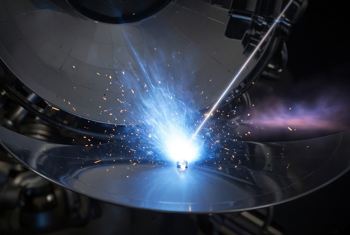
There is no EUV bulb. ASML's own description of the source is blunt. A carbon-dioxide laser fires two pulses at a fast-moving drop of tin, vaporising it, up to 50,000 times a second. The droplet is about 25 micrometres across, smaller than a hair, fired through the vacuum chamber at roughly 70 metres a second. The first pulse flattens it into a pancake so the second pulse couples into it efficiently. The pancake becomes a plasma. The plasma emits a broad spectrum. A multilayer collector selects the 13.5-nanometre slice the mirrors can use.
The film's more dramatic version is not invented, but it is the newer operating point. Engineers have moved from a double pulse toward a triple pulse on the high-power sources: pre-pulses that shape and rarefy the droplet, then a main pulse that ionises it. ASML and its source engineers described field sources above 500 watts of in-band EUV for the NXE:3800E generation, in a 2024 SPIE paper. That power is what lets the scanner move from the 160-wafer-an-hour class of the NXE:3600D to the 220-wafer-an-hour class of the NXE:3800E, quoted at a dose of 30 millijoules per square centimetre.
The temperature claim needs a label. Veritasium says each droplet is heated above 220,000 degrees, roughly forty times the surface of the Sun, the figure ZEISS publishes. The solar photosphere is about 5,800 kelvin, so forty times is about 230,000, and the figure is in the right band for a laser-produced tin plasma. ASML's own page puts the main pulse at about 500,000 kelvin. Either way it is a plasma temperature, not a bulk temperature of the machine. The chamber is not a star. A few tens of micrograms of tin are ionised for nanoseconds. The rest of the tool is a precision instrument that will be ruined if that tin lands on a mirror.
Debris is the unglamorous half of the source. Tin splashes. It coats the collector. Hydrogen flowing through the chamber at hundreds of kilometres an hour scavenges it, forming stannane gas that can be pumped away. Too little hydrogen and the mirrors die. Too much and the gas absorbs the EUV and the system overheats. Getting that balance, and getting the laser to hit every droplet, is why the source took longer than the optic. The film's line that the machine takes on the order of 150,000 laser shots a second and is not allowed to miss is the triple-pulse arithmetic: three shots on each of 50,000 droplets. It is a control problem, not a slogan.
One correction matters, because the film's chapter card invites it. The card reads "Nuclear Fusion To The Rescue." The plasma is not a fusion reactor. Tin ions emit the 13.5-nanometre line because of the way their electrons are stripped and recombine, not because hydrogen nuclei are fusing. No net energy is harvested. The laser puts far more energy in than the EUV that comes out. Conversion efficiency from laser to useful EUV is a few percent at best. The machine is a lamp of extraordinary inconvenience. It is not a power plant.
Mirrors that would be flatter than a country
Carl Zeiss SMT in Oberkochen makes the optics. The partnership is older than the product. ASML builds the scanner, the stages, the source integration and the control system. Zeiss builds mirrors whose figure error is measured in picometres. A picometre is a thousandth of a nanometre. ASML's own March 2024 description of the High-NA optic is the cleanest primary source: the biggest mirror is a metre across, with deviations no larger than tens of picometres, "like a playing card's thickness on Earth's surface."
The film's version is that claim, slightly loosened: scale the mirror to the Earth and the tallest bump is a playing card. Secondary accounts that scale the mirror to Germany and get a bump under a millimetre are the same tolerance in a different frame. Both are illustrations of a roughness specification, not a measurement you can repeat with a ruler. The engineering statement underneath them is solid. Mid-spatial-frequency roughness on these mirrors was driven from about 200 picometres RMS in the middle of the 2000s to about 50 picometres by the early 2010s, using computer-controlled polishing and ion-beam figuring. Individual mirrors for the projection optic take months to years. There is no second source at this specification.
The stages are the other half of the magic trick, and they are easier to under-describe. Printing a layer is not enough. The next layer has to land on it. ASML's 2024 reporting put matched-machine overlay on the NXE:3800E down to 0.9 nanometres. The High-NA production tool, the EXE:5200B, has been described at 0.7 nanometres. A silicon atom is roughly 0.2 nanometres across, and the lattice spacing is about 0.54 nanometres, so "a handful of atoms" is a fair popular translation of a 1-nanometre overlay. The film's "no more than five atoms" is that kind of translation. It is not a metrology specification, and it should not be quoted as one.
The accelerations are real and they are specific. The reticle and the wafer both scan during the exposure. High-NA descriptions from technical coverage put the wafer stage near 8 g and the reticle stage near 32 g. The film's "over 20 g, more than five times a Formula 1 car" is pointed at the reticle stage of the machine it tours. A Formula 1 car peaks around 5 g in braking. The comparison is fair as a scale marker. It is not a claim that the whole cabinet is shaking at 20 g. The stages are isolated. The cabinet stays put. The point of the number is that the positioning system has to know where a reticle is while that reticle is being thrown back and forth, and still land the image within a nanometre of the previous layer.
The company that did not walk away
ASML began in 1984 as a joint venture of Philips and ASM International, in a hut on a Philips site in Eindhoven, building steppers the market did not yet need. It did not invent lithography. It assembled a system no single firm could carry: Zeiss for the optics, Trumpf in Germany for the carbon-dioxide drive laser, Cymer in San Diego, later an ASML company, for the source, and a web of Dutch and European specialists for the stages, the vacuum and the handlers. The film's phrase for this, and the one ASML's own executives still use, is that the tool is an act of extreme cooperation. That is accurate. It is also why the monopoly has lasted. A rival does not have to copy one machine. It has to copy a supply chain that took thirty years to synchronise.
The commercial crossing came later than the laboratory crossing. A working EUV prototype in the early 2000s could print features and could not print them fast enough to matter. Power sat in the single-digit watts when the fab wanted tens, then in the tens when the fab wanted a hundred. By 2014 the source had reached the 100-watt region. By then, multi-patterning on 193-nanometre immersion had improved, and the bar moved to 200 watts and 125 wafers an hour. The film's account of that moving target matches the public record. Orders for production tools began in earnest around 2016. High-volume insertion followed at the 7-nanometre and 5-nanometre logic generations.
TSMC, Samsung and Intel are the logic customers that matter, and the DRAM makers, SK Hynix, Samsung and Micron, now print their densest memory layers on EUV as well. ASML does not publish a customer-by-customer tool count in the way a gossip column would like, but it does not need to. No other firm ships an EUV scanner.
Export control sits on top of the monopoly. The Netherlands, under its own rules and under U.S. pressure, does not license EUV tools for China. That is not a rumour. It is policy, and it is why the most advanced AI accelerators are printed in Taiwan, South Korea and the United States, not in a mainland Chinese fab. Older deep-ultraviolet tools have been restricted in later rounds as well. The strategic fact is simple. The machine that looks alien is also a chokepoint, and it sits in a town of about 45,000 people.
The money is no longer a start-up story. ASML's 2025 net sales were 32.7 billion euros, up 15.6 percent, with a gross margin of 52.8 percent, per its 2025 annual report. EUV system sales and a large installed-base business, field upgrades of the NXE:3800E in particular, carried the year. The company returned 8.5 billion euros to shareholders. A monopoly on the critical exposure tool, sold to a handful of chipmakers who cannot design around it, has a particular kind of income statement.
High-NA, and what four hundred million dollars actually buys
The film's four-hundred-million-dollar figure is the number that escaped into every recap, and it needs a fence around it. ASML does not publish a list price. Trade reporting puts a current 0.33-NA tool, the NXE class, in a band around 150 to 200 million euros. The same reporting puts the 0.55-NA High-NA tool, the EXE class, near 350 to 400 million dollars, and Bloomberg has quoted a figure upwards of 350 million euros. The video is talking about the new machine. Quoting 400 million dollars as the price of "the" EUV scanner erases a generation.
What the new machine changes is the numerical aperture, not the wavelength. NA goes from 0.33 to 0.55. ASML's stated resolution goes from 13 nanometres to 8. The optic is anamorphic: 4x shrink in one axis, 8x in the other, so that a standard six-inch reticle can still be used. The field printed in one exposure is halved. The mirrors are larger. MIT Technology Review, touring the tool in 2026, described a projection system weighing 12 tons, seven times the previous optic. Industry descriptions of the full High-NA scanner put the mass near 150 tonnes and the shipping load near 250 crates, with installation measured in months and headcount in the hundreds. Treat the crate count and the headcount as industry-reported, not as a line in an ASML datasheet.
The first High-NA tool, an EXE:5000, was delivered in December 2023 for process development. Intel took the early units in Oregon. TSMC and Samsung took R&D tools. A joint ASML–imec High-NA lab operates in Veldhoven. The production scanner, the EXE:5200B, first shipped in early April 2025, per ASML's 2025 annual report, with a stated throughput of 175 wafers an hour, a 60 percent productivity step over the EXE:5000. Intel has been the first to put High-NA layers into a shipping logic product path. On 15 July 2026 ASML said Intel was the first to ship high-volume logic made with the tools, on selected layers of Intel 18A, a 2-nanometre-class process. TSMC has been public about not needing High-NA for its first A14-class node. That split is the tell. High-NA is a real tool. It is not yet the only way to print a leading-edge chip.
Spec | NXE:3800E (0.33 NA) | EXE:5200B (0.55 NA) |
|---|---|---|
Wavelength | 13.5 nm | 13.5 nm |
Resolution (ASML) | 13 nm | 8 nm |
Throughput | Up to 220 wafers/hour at 30 mJ/cm2 | 175 wafers/hour at 50 mJ/cm2 |
Overlay | Matched-machine down to 0.9 nm | Reported 0.7 nm on the production SKU |
Light source | Laser-produced tin plasma, field sources above 500 W | Same physics, higher-power source shared with NXE:3800E |
List price | Not published. Industry band roughly 150–200 million euros | Not published. Reported band about 350–400 million dollars |
Sources: ASML product pages for wavelength, NA and resolution; ASML 2024 annual-report figures for NXE:3800E throughput and overlay; Bits&Chips, July 2025, for the EXE:5200B shipment and 175 wafers/hour; SPIE 2024 for the >500 W source. Prices are industry-reported bands. ASML does not publish a list price.
The reason a fab buys it is not the brochure resolution. A single High-NA exposure can replace a multi-patterned Low-NA sequence on the tightest layers, cutting process steps, cycle time and the overlay risk that comes from splitting one layer into several masks. Whether that trade pays depends on dose, on the half-field, and on how many layers actually need 8-nanometre resolution. Intel's decision to dual-qualify selected layers, rather than flip an entire process onto the new tool, is the adult version of the story.
The other alien machine: a chip the size of a dinner plate
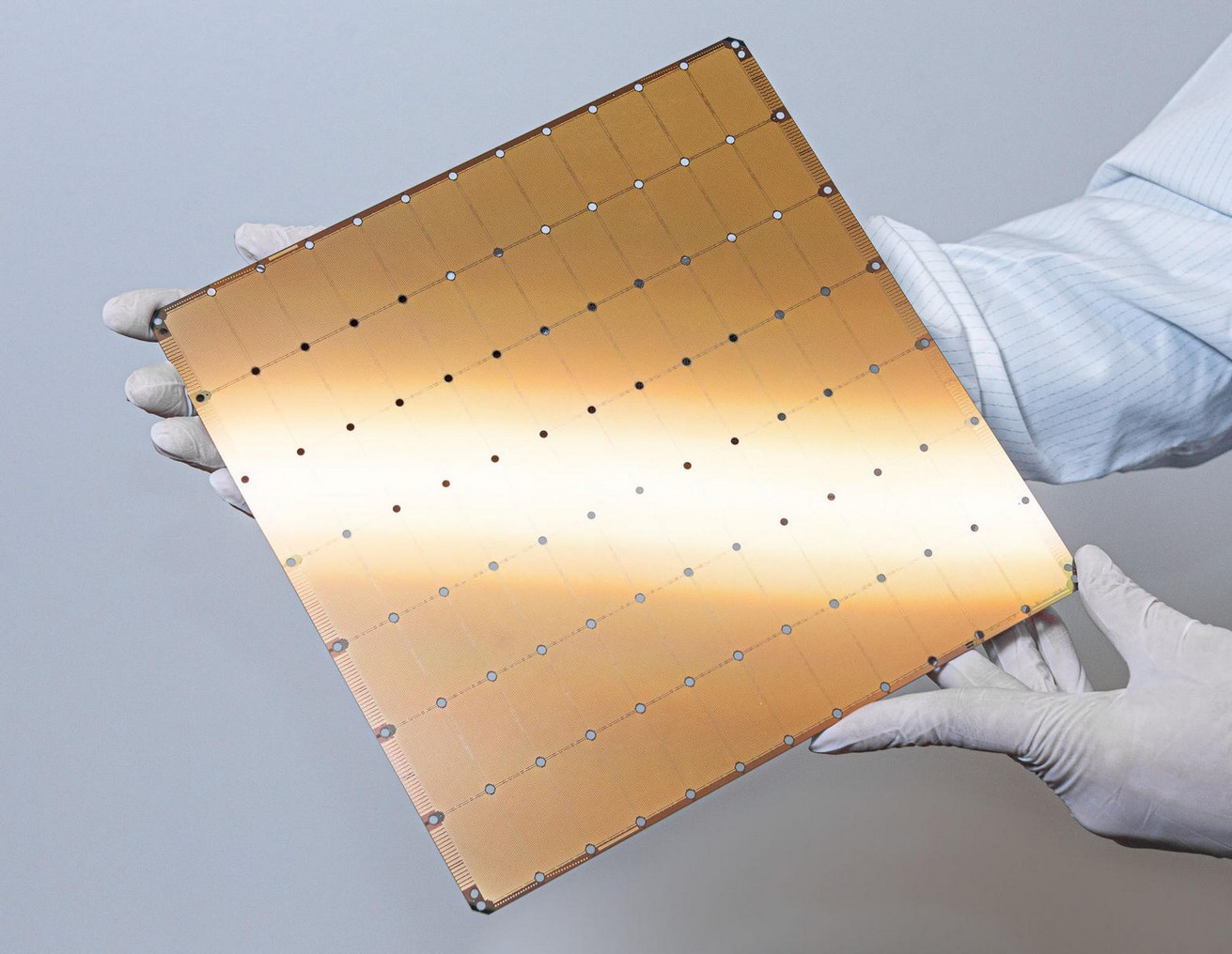
Lithography is not the only object in this stack that fails a sanity check. Cerebras took the opposite bet from the rest of the industry. Everyone else saws the wafer into dies, throws away the dies that fail, and stitches the good ones back together on a package. Cerebras keeps the wafer. The Wafer-Scale Engine 3, launched in March 2024 and built on TSMC's 5-nanometre process, is a single square of silicon of 46,225 square millimetres. Cerebras states 4 trillion transistors, 900,000 cores aimed at sparse linear algebra, 44 gigabytes of on-chip SRAM, 21 petabytes a second of on-wafer memory bandwidth, and 125 petaflops of AI compute. Those are vendor figures. They have been repeated by independent technical outlets without a contradicting teardown, which is as much independent checking as a wafer you cannot easily buy will get.
The point of the object is distance. On a GPU, a weight moves off the die, across a package, into a stack of high-bandwidth memory, and back. On a wafer-scale engine the memory is SRAM on the same silicon as the arithmetic. The bandwidth number is what you get when you stop leaving the chip. The cost is yield, power delivery and a cooling problem the size of a serving platter. Cerebras is not the volume path for AI. NVIDIA's packaged GPU is. The wafer-scale engine belongs here because it is the same impulse as the EUV scanner: when the ordinary object cannot do the job, build an object that looks wrong and make the physics agree.
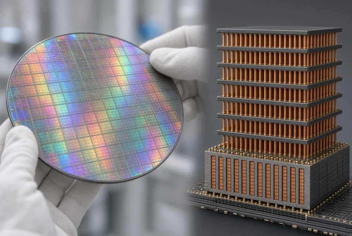
The volume path has its own wrong-looking object. High-bandwidth memory is a skyscraper. Eight, twelve, now sixteen DRAM dies are stacked, drilled with through-silicon vias, and parked beside the logic die on an interposer. NVIDIA's GB200 NVL72 rack holds 72 Blackwell GPUs and 36 Grace CPUs. It pools 13.4 terabytes of HBM3e across the rack, with 130 terabytes a second of all-to-all NVLink inside the cabinet, per NVIDIA. The successor GB300 NVL72, the Blackwell Ultra rack, keeps the 72-GPU domain and raises pooled HBM3e to about 20 terabytes. Its chips run at a TDP around 1,400 watts, and the rack draws in the 132 to 140 kilowatt band, with peaks near 155 kilowatts in integrator specifications. A decade ago a dense rack was a 7-kilowatt problem. The AI rack is twenty times that, liquid-cooled, because air cannot move the heat.
The rack that is one computer
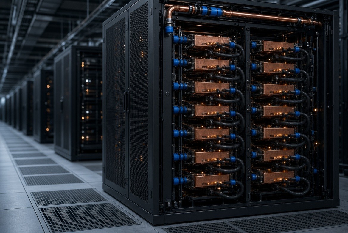
The interesting decision in the NVL72 is not the part count. It is the wiring. Extending NVIDIA's NVLink across the rack, rather than stopping at the board, lets the 72 GPUs be programmed as one accelerator. The tax is paid in transceivers, in copper, and in power. Independent estimates have put the optical and electrical interconnect alone at a meaningful fraction of the rack budget. The cooling loop is no longer optional. NVIDIA's reference designs take warm water in, around 32 to 45 degrees Celsius, and return it hotter. Integrator sheets for the GB300 rack quote a fully loaded mass around 1.5 tonnes and a coolant flow up to 130 litres a minute. The cabinet is a heat exchanger that happens to compute.
Behind the rack, the building has changed shape. A hall of NVL72-class racks is a power-delivery project. Substations, on-site generation, and arguments with utilities are now on the critical path of model training, alongside the GPU purchase order. Water is the other constraint. Direct-to-chip liquid cooling cuts the room-level air load, and it concentrates the water and the chemistry problem into a plant the public does not tour. The film never leaves the cleanroom. The AI system does not fit in the cleanroom. It fits in a windowless hall whose alien feature is the busbar.
Packaging is the quiet third machine. TSMC's CoWoS family, and the competing 2.5D and 3D flows at Samsung and Intel, are what let a logic die sit next to six or eight HBM stacks with a wiring density a conventional substrate cannot provide. The interposer is itself a silicon wafer, patterned on older lithography, because the features are larger and the area is not. The shortage of 2023 and 2024 was not only a shortage of GPUs. It was a shortage of the packaging line that turns a GPU die into a GPU. A fab can print a die it cannot ship. That bottleneck has eased as capacity has been added. It has not disappeared, and it moves with every jump in HBM stack height.
What the cleanroom is actually cleaning
The film's cleanroom sequence is the right place to end the tour, because the room is part of the machine. A particle a tenth of a micrometre across is a boulder on a 13-nanometre feature. ASML and its customers run the scanner in air that is specified in single-digit particles per cubic metre at that size, orders of magnitude cleaner than a surgical theatre. The suit is not costume. Skin, breath and the seam of a glove are contamination sources. The wafer handler exists so that a person does not touch the wafer.
The same intolerance shows up in the overlay loop. The scanner measures each wafer and corrects the optic and the stage for that wafer. A process that could not do this would print beautiful features in the wrong place, which is a dead chip with extra steps. The NXE:3800E's selling point, in ASML's own words, is that it combines in-situ measurement with per-wafer correction, on top of the higher-power source and the faster stages shared with the High-NA platform. Productivity and placement are the same problem seen from two sides.
It is worth being plain about who can buy the result. A handful of companies run these tools in volume: TSMC, Samsung and Intel in logic, SK Hynix, Samsung and Micron in memory. Their customers, NVIDIA, AMD, Broadcom and the hyperscalers designing their own accelerators, design to a process those fabs can print. The diffusion of AI is wide. The diffusion of the machine that prints AI is not. That concentration is the fact underneath every export-control argument, and it will not be diversified by a software release.
The chain, mapped
The film tours one machine. KXCO's AI Sector Ontology maps the chain around it as typed claims, each carrying its source, its confidence and the dates it held. As of 7 October 2026 it holds 413 entities and 937 current relationships, and it keeps superseded claims rather than overwriting them, so the record can be read as it stood on any past date.
ASML sits at the root of the semiconductor side of that graph, one of nine nodes the ontology flags as chokepoints. Its inbound edges are the ones described above: Zeiss, recorded as the sole supplier of EUV optics to ASML, and Trumpf, the sole supplier of its EUV laser sources. Its outbound edges run to TSMC, Samsung, SK Hynix, Intel and Rapidus as their EUV supplier, and to Low-NA and High-NA EUV as the only maker of both. Both scanner generations are flagged as chokepoints in their own right. So are SK Hynix and Samsung Electronics, on the memory side, for their share of the high-bandwidth memory every accelerator needs.
The same record carries the money. ASML reported 9.3 billion euros of second-quarter net sales at a 54.0 percent gross margin on 15 July 2026, and raised its 2026 outlook to between 43 billion and 45 billion euros, per its second-quarter results. China is about a fifth of 2026 revenue, per CNBC, and it buys deep-ultraviolet tools only, because EUV has never shipped there. Each of those claims sits in the ontology with its source attached, beside the Cerebras, Nvidia, Broadcom and memory-maker nodes covered above.
The use of the awe
The temptation with a machine like this is to file it under wonder and move on. That wastes the fact. The wonder is the point, and the point is narrow. A civilisation that can hit a 25-micrometre droplet of tin fifty thousand times a second, with a laser it is not allowed to miss, and bounce the resulting light off a mirror flatter than any natural surface, can print the switches that make a language model possible. It can also fail to print them. The tool is singular, slow to build, slower to copy, and already an instrument of foreign policy.
AI will keep being described as software. The software is real. The weights are real. The product people touch is a chat window. Under the window is a rack that looks like an engine room, under the rack is a package that looks like a skyscraper, and under the package is a wafer that was exposed, one layer at a time, by a bus-sized vacuum chamber in a Dutch cleanroom, firing a star the size of a speck of dust. That is the machine. It is not alien. It is ours. It only looks like it came from somewhere else because nothing in ordinary experience prepares you for the tolerances.
Moore's law was never a law. It was a budget for difficulty, renewed every two years by people who built the next tool before the last one had paid for itself. EUV is the renewal that almost did not happen. High-NA is the renewal underway now, bought by the fab that needs it first and watched by the fabs that can wait a node. The models will get larger. The droplets will keep falling, fifty thousand a second, in a room no customer of the model will ever see.
Notes
Sulli Yost, Casper Mebius and Derek Muller, "The Closest Thing We Have to Alien Technology," Veritasium, YouTube video, 31 December 2025, youtube.com/watch?v=MiUHjLxm3V0. Also released under the title "The Ridiculous Engineering of the World's Most Important Machine." With thanks to Marc Assinck, Jos Benschop, Jan van Schoot and Jayson Stewart of ASML, per the film's description.
ASML, "TWINSCAN NXE:3800E," product page, Veldhoven, accessed October 2026, asml.com. Wavelength 13.5 nm, numerical aperture 0.33, resolution 13 nm, throughput up to 220 wafers an hour at 30 mJ/cm2.
ASML, "EUV lithography systems," product pages for the TWINSCAN EXE family, Veldhoven, accessed October 2026, asml.com. EXE systems: 13.5 nm, numerical aperture 0.55, resolution 8 nm. Source: a CO2 laser fires two pulses at a drop of tin, up to 50,000 times a second.
ASML, Annual Report 2025, Veldhoven, 2026, sec.gov. Net sales 32.7 billion euros, gross margin 52.8 percent, 8.5 billion euros returned to shareholders.
ASML (@ASMLcompany), "The biggest mirror in our High NA EUV system is 1 meter across but with deviations no larger than tens of picometers. That's like a playing card's thickness on Earth's surface," X, 18 March 2024, x.com.
Klaus Hummler, Qiushi Zhu, Keegan Behm et al., "High-power EUV light sources (>500 W) for high throughput in next-generation EUV lithography tools," Proceedings of SPIE 12953 (10 April 2024): 129530V, doi.org/10.1117/12.3010463.
Paul van Gerven, "ASML ships first high-NA EUV production scanner," Bits&Chips, 23 July 2025. First EXE:5200B, 175 wafers an hour.
Clive Thompson, "The $400 million machine powering the future of chipmaking," MIT Technology Review, 23 June 2026, technologyreview.com.
Cerebras Systems, Wafer-Scale Engine 3 launch specifications, March 2024. Time, "Best Inventions of 2024."
NVIDIA, GB200 NVL72 and GB300 NVL72 system descriptions; integrator specifications from Supermicro, HPE and SemiAnalysis InferenceX, 2025–2026.
Marc Hijink, Focus: The ASML Way (Amsterdam: Balans, 2023). Jayson Stewart, "The Tiny Ultraviolet Plasma That Powers Advanced Chipmaking," IEEE Spectrum.
ASML, "ASML reports 9.3 billion euros total net sales and 2.9 billion euros net income in Q2 2026," 15 July 2026, sec.gov.
KXCO, AI Sector Ontology, as of 7 October 2026, kxco.ai/ontology-live.
Stocks mentioned: $ASML (NASDAQ), $TSM (NYSE), $NVDA (NASDAQ), $INTC (NASDAQ), $MU (NASDAQ), $AMD (NASDAQ), $AVGO (NASDAQ) and $CBRS (NASDAQ).
Shayne Heffernan, Ph.D., is the founder of Live Trading News, the KnightsBridge Group, Knightsbridge Law and the KXCO.ai ecosystem spanning post-quantum cryptography, identity, attestation and enterprise ontology.

There Is No AI Bubble
There is no AI bubble. A bubble is capacity nobody uses, demand nobody signs for and a glut when the building stops. KXCO's AI sector ontology, refreshed on 7 October 2026, finds the reverse: adoption rising on six independent measures, about $2.35tn of contracted backlog at the four largest sellers of compute per their own reports, and supply rationed at every layer. It keeps the bear case in the same record, 20 circular capital claims, and answers it.

Weekly Market Outlook: Fed Minutes, Anthropic and OpenAI IPOs, Gold, Bitcoin, FX
The Fed raised rates in September and payrolls rose 29,000, per the Labor Department. This week the FOMC minutes, three Treasury auctions and a 10-year near 5.3 percent test that gap. Anthropic's IPO clock runs toward a 14 October investor day while OpenAI's chief executive says not 2026. Gold sits 26 percent below its record, bitcoin near $85,500, the dollar up three weeks running. Two knowledge graphs from KXCO's records map the IPO backers and the FDA board.
Thoughts on Thinking in an AI World
A model will write an answer about anything in seconds. What an AI world makes scarce is everything around the answer: what you believed last month and why you changed it, the link between fields nobody reads together, and a decision a named person can stand behind. Three knowledge-graph exhibits from the KXCO record show each one, from a reported Nvidia deal that became a signed 8-K to a war five links from a data centre.
AI Development: The Token Got Cheaper, the Building Did Not
The useful fact on 28 September is a split, not a benchmark. Gartner puts 2026 AI spending at $2.67 trillion, and 56 percent of it is infrastructure against about 1 percent on the models. Inside one week the frontier cut the price of a token in half, Nvidia signed for the shelf the open weights sit on, and three closed labs proposed to run the test. What shipped, what it costs and where the money goes, with the AI sector checked against KXCO Ontology Live.
Every story, signed and delivered.
Subscribe to the kxco channel and get the headline, the AI-written key takeaways, and the chain-anchor link the moment we publish. Audio versions and per-ticker subscriptions arrive in the next iteration.